Combinational Logic & SystemVerilog — First Contact
Rodolfo Azevedo
Institute of Computing, University of Campinas (UNICAMP), Brazil
rodolfo.azevedo@unicamp.br
http://www.ic.unicamp.br/~rodolfo/mo801
Goal of this class
Module 1, Class 1: from logic gates to SystemVerilog — and a first circuit running on real hardware.
This class assumes you have seen logic gates before. The goal is not to re-teach them — it is to connect what you already know to the language (SystemVerilog) and tools (OSS CAD Suite) we will use for the rest of the course.
At the end of this class, you should be able to:
- Describe the behavior of logic gates (AND, OR, NOT, XOR, NAND, NOR) using truth tables and Boolean equations.
- Write synthesizable SystemVerilog modules with
assign, port declarations, and module instantiation. - Apply Boolean algebra and De Morgan's theorem to simplify combinational logic.
- Use vectors, concatenation, and width casting in SystemVerilog to handle multi-bit signals.
- Synthesize a combinational circuit and load it onto the Tang Nano 9K FPGA.
Why start here?
The end goal of this course is to run a keyword-spotting AI on a processor you built from scratch. That processor will be tens of thousands of gates. Every one of them obeys the same rules as the AND gate on this slide.
Understanding hardware at the gate level is what separates someone who uses an FPGA from someone who builds what runs on it.
The digital abstraction
Real circuits deal in voltages. We simplify them to two values:

- 0 → low voltage (GND, typically 0 V)
- 1 → high voltage (\(V_{DD}\), typically 1.8–3.3 V in modern devices)
This works because logic families define noise margins: a range of voltages around each level that are still reliably interpreted as 0 or 1. As long as noise stays within the margins, the digital abstraction holds — we never have to think about voltages again.
The Gowin GW1NR-9C on the Tang Nano 9K is a 3.3 V device; its I/O banks operate at 3.3 V or 1.8 V depending on pin configuration.
Logic gates — the vocabulary
| Gate | Symbol (text) | Boolean | Behaviour |
|---|---|---|---|
| NOT | ~a |
\(\bar{a}\) | Inverts the input |
| AND | a & b |
\(a \cdot b\) | 1 only when both inputs are 1 |
| OR | a \| b |
\(a + b\) | 1 when at least one input is 1 |
| NAND | ~(a & b) |
\(\overline{a \cdot b}\) | Inverted AND |
| NOR | ~(a \| b) |
\(\overline{a + b}\) | Inverted OR |
| XOR | a ^ b |
\(a \oplus b\) | 1 when inputs differ |
| XNOR | ~(a ^ b) |
\(\overline{a \oplus b}\) | 1 when inputs are equal |
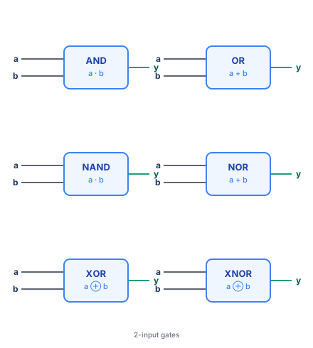
These operators appear in SystemVerilog exactly as shown in the Symbol (text) column — so the language and the circuit description are already the same notation.
Truth tables and Boolean equations — example
Seat-belt alert: a car sounds an alarm (\(S\)) if the ignition is on (\(K\)) and either the driver (\(D\)) or passenger (\(P\)) is not wearing a belt.
| \(K\) | \(D\) | \(P\) | \(S\) |
|---|---|---|---|
| 0 | × | × | 0 |
| 1 | 0 | 0 | 1 |
| 1 | 0 | 1 | 1 |
| 1 | 1 | 0 | 1 |
| 1 | 1 | 1 | 0 |
This is a combinational circuit: the output depends only on the current inputs, with no memory of the past.
From equation to SystemVerilog — immediately
module/endmodule— the building block of a SystemVerilog designinput/output— the ports of the module, visible from the outsideassign s = ...— continuous assignmentsis permanently wired to this expression- Change any input,
supdates instantly (in the model) or within nanoseconds (in real hardware) - The SV operators (
&,|,~) are exactly the Boolean operators from the previous slide. logic— the type for almost everything in this course- A 4-state type:
0,1,x(unknown),z(undriven) - For synthesizable logic, you will see only
0and1
Boolean algebra — the rules you already know
These identities let you simplify circuits (fewer gates = smaller, faster hardware):
| Identity | AND form | OR form |
|---|---|---|
| Identity | \(a \cdot 1 = a\) | \(a + 0 = a\) |
| Null | \(a \cdot 0 = 0\) | \(a + 1 = 1\) |
| Idempotent | \(a \cdot a = a\) | \(a + a = a\) |
| Complement | \(a \cdot \bar{a} = 0\) | \(a + \bar{a} = 1\) |
| De Morgan | \(\overline{a \cdot b} = \bar{a} + \bar{b}\) | \(\overline{a + b} = \bar{a} \cdot \bar{b}\) |
| Distributive | \(a(b+c) = ab + ac\) | \(a + bc = (a+b)(a+c)\) |
De Morgan is the most important: it explains why NAND and NOR are universal gates (any function can be built from NAND alone), and why we write ~(a & b) instead of ~a | ~b — they are the same circuit.
Vectors: multi-bit signals
A single logic is one wire. A vector is a bundle of wires:
Operators apply bitwise across vectors:
Reduction operators collapse a vector to one bit:
Number literals
- Default base is decimal if no prefix is given:
8'd255=255=8'b11111111 b= binary,h= hex,d= decimal,o= octal- Width is optional:
8'hFF=hFF=255=8'b11111111 '0and'1are width-agnostic:'0= all-zeros,'1= all-ones, whatever the context width is.- Notice the difference between
0(decimal 0) and'0(all-zeros, width determined by context),1(decimal 1) and'1(all-ones, width determined by context) xandzare also width-agnostic:'x= all unknown,'z= all undriven
Concatenation
{a, b} joins two vectors into one — essential for building wider signals:
The {N{expr}} replication syntax is used constantly for sign extension — you will write it dozens of times in Project 1's immediate-reconstruction logic.
Sign extension is the process of increasing the width of a binary number while preserving its value, typically by replicating the most significant bit.
Width casting: N'(expr)
When expressions mix different bit-widths, SystemVerilog silently zero-extends or truncates the shorter operand. This is a frequent source of subtle bugs.
The fix: use N'(expr) to make the intended width explicit:
Key rules:
- Use
N'(expr)whenever the right-hand side has a different bit-width from the target — especially withlocalparamarithmetic. '0extends to all-zeros matching the context width;'1extends to all-ones.- Explicit casts make both code and synthesis reports easier to read, and prevent Verilator
-Wallwarnings that hide real bugs.
Modules and ports — the building block
A module is a black box: visible from the outside only through its ports. Inside can be any logic; the rest of the design does not care.
Instantiation — using a module inside another
.port(signal)— always prefer named connections over positional; self-documenting and survives port-order changes.logic ab— an internal signal connecting the two instances, visible only insideand3.

A more interesting example: majority function
Output is 1 when at least 2 of 3 inputs are 1. The Boolean equation (from SOP):
Equivalently with De Morgan (using only NAND):
Both descriptions produce the same circuit — the synthesis tool picks the implementation.
Toolchain express — before touching the board
You need four tools from the OSS CAD Suite (one installer, all platforms):
Minimal project layout:
To synthesize and load: make load (full Makefile in M01A06; for now, use the Lab 2 starter template).
Lab 2 walks through the full setup step by step — complete it before the next class so you can do Lab 3 on the board.
The Tang Nano 9K: your hardware target
- FPGA: Gowin GW1NR-9C — 8,640 LUTs, 6,480 FFs, 468 Kbit BRAM, 64 Mbit external PSRAM.
- LUT = lookup table, implements any combinational function of N inputs
- FF = D flip-flop, registered state
- BRAM = block RAM, on-chip memory, inferred from
logicarrays See M01A06 for the full primitives table.
- On board: 27 MHz oscillator, 6 user LEDs (active-low), 2 push buttons, UART via USB.

Your job today
- Synthesize a combinational circuit whose inputs are the 2 buttons and whose outputs are some of the 6 LEDs.
Board exercise: logic functions on buttons and LEDs
- Notice that the LED logic maps directly to the Boolean expressions from the first slides.
- Synthesize with
make load(Yosys → nextpnr → openFPGALoader) and press the buttons. You are observing real combinational hardware — no CPU, no code.
Next class
Combinational Building Blocks: multiplexers, decoders, comparators — and always_comb and case in SystemVerilog, the tools for describing more complex combinational logic cleanly.