Sequential Logic & SystemVerilog
Rodolfo Azevedo
Institute of Computing, University of Campinas (UNICAMP), Brazil
rodolfo.azevedo@unicamp.br
http://www.ic.unicamp.br/~rodolfo/mo801
Goal of this class
Module 1, Class 3: latches, flip-flops, registers, counters — and always_ff.
Combinational circuits compute functions of current inputs. Sequential circuits also remember the past. This class introduces the element that makes memory possible: the flip-flop — and the SystemVerilog construct
always_ffthat describes it.
At the end of this class, you should be able to:
- Explain the D flip-flop's setup time, hold time, and propagation delay, and why violating them causes metastability.
- Write synchronous sequential circuits using
always_ffwith non-blocking assignments. - Implement registers, counters, and the two-process pattern in SystemVerilog.
- Apply a two-FF synchronizer to safely bring asynchronous inputs into a synchronous design.
- Analyze clock timing constraints (t_pcq + t_comb + t_su) and interpret nextpnr timing reports.
Why we need memory: the latch
Consider a traffic light controller. The output (which light is on) depends not only on a push-button but also on which state the light was in before. That is sequential behaviour — the circuit needs to remember something.
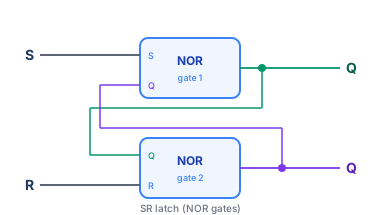
The simplest memory element is the SR latch (Set-Reset), built from two cross-coupled NAND gates:
| S | R | Q (next) |
|---|---|---|
| 0 | 0 | Q (hold) |
| 0 | 1 | 0 (reset) |
| 1 | 0 | 1 (set) |
| 1 | 1 | undefined |
The undefined state and level-sensitive (not edge-triggered) behaviour make raw latches difficult to use reliably in synchronous designs. In practice, we use flip-flops.
The D flip-flop: edge-triggered memory
A D flip-flop (DFF) samples its input \(D\) at the rising edge of the clock and holds it until the next rising edge:

- Setup time (\(t_{su}\)): \(D\) must be stable before the rising edge.
- Hold time (\(t_h\)): \(D\) must stay stable after the rising edge.
- Propagation delay (\(t_{pcq}\)): time from clock edge to valid \(Q\).
Violating setup or hold time causes metastability — the flip-flop output is unpredictable. This is why you cannot connect two independent clock domains directly without a synchronizer.
The DFF is the fundamental building block of all synchronous digital design. Every register, every FSM state, every pipeline stage is a collection of DFFs.
The two-flip-flop synchronizer
Any signal that crosses a clock domain boundary — or comes from outside the chip entirely (button press, UART RX) — can arrive at any phase relative to the destination clock. If it violates the DFF's setup or hold time, the output may never settle to a valid 0 or 1: this is called metastability.
Solution: cascade two DFFs clocked by the destination domain.
- The first FF can go metastable, but has a full clock period to settle before stage 2 samples it.
- Rule: every asynchronous input — button, UART RX line, any cross-domain signal — must pass through a synchronizer before any logic uses it.
- Two FFs suffice for most FPGA frequencies (≤ 100 MHz). Very high-speed designs use three.
Level detection vs. edge detection
Level detection: logic acts every cycle that a signal holds a value.
Edge detection: logic acts exactly once, on the transition. Implemented by comparing the current value to a one-cycle-delayed copy:
Why it matters for UART RX: * The receiver must detect the falling edge of the START bit, then count half a bit-period to reach the centre of bit 0. * Level detection would re-trigger the receiver on every cycle the line is low. * Edge detection fires once; a counter then times out to the sample point.
Common bug: using level detection for a button → an action (e.g., counter increment) repeats millions of times per second while the button is held.
always_ff — describing flip-flops in SystemVerilog
Key rules for always_ff:
* Use non-blocking assignment <= — never = inside always_ff.
* The sensitivity list must be @(posedge clk) (or @(negedge clk) for falling-edge). Tools reject other patterns.
* The synthesis tool maps this directly to a flip-flop primitive in the target technology.
Synchronous vs. asynchronous reset
Both styles are common; your project's choice must be consistent throughout:
- Synchronous reset: simpler timing analysis, easier to synthesize; requires a clock edge to release reset. Preferred for most student designs.
- Asynchronous reset: can reset even with no clock running; adds a separate path through the flip-flop's
rstpin. '0is the aggregate zero literal — fills the entire left-hand side with zeros, regardless of width. Equivalent to4'b0000for a 4-bit signal but works for any width.
Non-blocking assignment — why it matters
Wrong: produces a shift register in simulation, but models wrong hardware intent with blocking '='
Correct: both sample simultaneously at the clock edge
The rule is simple and absolute
<=(non-blocking) insidealways_ff— models registers: all right-hand sides are evaluated first using old values, then all assignments happen simultaneously.=(blocking) insidealways_comb— models wires: evaluation proceeds top-to-bottom like sequential software.
Mixing the two inside one block is a synthesis error.
Registers: N flip-flops sharing a clock
An \(N\)-bit register is \(N\) DFFs with a shared clock and reset:
With an enable signal (load only when en is high):
This pattern — register with synchronous reset and enable — is the template for every register in the RV32I datapath: PC, IR, MDR, ALUOUT, and the 32 general-purpose registers.
Shift register
A serial-in, serial-out (SISO) shift register delays a 1-bit signal by \(N\) clock cycles:
{sr[DEPTH-2:0], d}is concatenation: drop the MSB (which exits asq) and append the new input at the LSB.- After \(N\) cycles of stable input
d,qequalsd. This is a \(N\)-cycle pipeline delay.
Applications in this course
- UART TX: the transmitter loads an 8-bit byte into a shift register and shifts one bit per baud period onto the TX line (M03A03).
- SPI: master and slave exchange bits simultaneously through a shared shift register pair.
- Depth-1: a single DFF — the atomic pipeline stage. Every pipeline register in Project 3's accelerator is a shift register of depth 1.
Counters
A synchronous counter increments its value every clock cycle:
- A 25-bit counter on a 27 MHz clock overflows every \(2^{25} / 27\,\text{MHz} \approx 1.24\) seconds — slow enough to see on an LED.
- The most significant bit
count[24]toggles at half that rate (once every ~0.62 s), giving a visible blink. - Asynchronous counters (each FF clocked by the previous FF's output) exist but are harder to time and not used in synchronous designs.
In-class exercise — sequential circuits
Extend the basic counter with load and en control inputs:
rst |
load |
en |
Behaviour |
|---|---|---|---|
| 1 | × | × | Synchronous reset → 0 |
| 0 | 1 | × | Load the value on d |
| 0 | 0 | 1 | Increment by 1 |
| 0 | 0 | 0 | Hold current value |
Trace on paper (start count = 4'h3): apply load=1, d=4'hA; then en=1 for 3 cycles; then en=0 for 1 cycle. Write count after each clock edge.
Expected sequence:
3 → A → B → C → D → D. Any difference? Check the priority of yourif/else ifbranches — the order matters.
The two-process pattern
Separating state storage from next-state logic keeps code readable and synthesizable:
This two-process pattern is the standard template for FSMs (next class) and datapath components. The always_ff block is always trivial; all the interesting logic lives in always_comb.
Timing: clock period and maximum frequency
The clock period must be long enough for the longest combinational path between two registers:
where
- \(t_{pcq}\) is the flip-flop propagation delay
- \(t_{comb}\) is the combinational delay through logic
- \(t_{su}\) is the setup time of the destination flip-flop.
After place-and-route, nextpnr reports the worst negative slack (WNS): * WNS ≥ 0 → timing met at the requested frequency * WNS < 0 → timing violated; reduce frequency or shorten the critical path
The Tang Nano 9K runs at 27 MHz. A minimal RV32I core easily meets 27 MHz. But if you add a deep combinational path (e.g., a multi-cycle multiplier in the ALU), you may need to pipeline it.
Board exercise — LED blink counter
Synthesize and load. You should see LEDs blinking at different rates — a direct visualization of binary counting.
Signal naming convention
Consistent names make code readable and catch bugs at review time. The conventions below are used throughout this course and match industry practice.
| Signal | Convention | Example | Notes |
|---|---|---|---|
| Clock | clk |
clk, clk_fast |
One clock per domain; prefix if multiple |
| Reset, active-high | rst |
rst |
Asserted when 1; released on clock edge (sync) |
| Reset, active-low | rst_n |
rst_n |
_n suffix = active-low; 0 means reset |
| Enable | en or *_en |
uart_en, cnt_en |
Allows operation when 1 |
| Write enable | we |
regfile_we |
Enables a write on the next rising edge |
| Chip select | cs_n |
sram_cs_n |
Active-low select; common in memory interfaces |
| Data valid | valid |
rx_valid |
Producer asserts: "this data is good right now" |
| Ready | ready |
tx_ready |
Consumer asserts: "I can accept data right now" |
| Load / latch | load |
ir_load |
Capture input into a register this cycle |
| Done / done flag | done |
mult_done |
One-cycle pulse when an operation completes |
| Next-state copy | *_next |
state_next, pc_next |
Combinational; wired to the <= in always_ff |
Signal naming convention (continued)
Active-low signals
- Carry the
_nsuffix and are driven 0 to assert - The Tang Nano 9K buttons and LEDs are active-low (
btn[0]pressed → 0;led[0]on → 0)
Edge convention in names
posedge clk= rising-edge clocked (default)negedge clk= falling-edge- Write
clk_nonly when referring to the inverted clock line itself, not to falling-edge sensitivity
Next class
FSMs in SystemVerilog: Moore and Mealy machines, state encoding with typedef enum, and typedef struct packed for grouping control signals — exactly the patterns you will use in Project 1's control FSM.