AI Accelerators: Architecture Overview
Rodolfo Azevedo
Institute of Computing, University of Campinas (UNICAMP), Brazil
rodolfo.azevedo@unicamp.br
http://www.ic.unicamp.br/~rodolfo/mo801
Goal of this class
Module 5, Class 1: from profile to architecture — what production accelerators look like and where your design fits.
You have a spec (M04A04) and a profiling baseline (M04A03). This class puts both in context: what does a real ML accelerator look like, and which ideas are directly applicable at the Tang Nano 9K scale?
At the end of this class, you should be able to:
- Describe the ML hardware taxonomy (CPU, FPGA, DSP, ASIC NPU) and position each on the flexibility–efficiency trade-off.
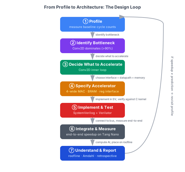
- Explain the design loop: profile → architecture → implement → measure → iterate.
- Apply the roofline model to predict the attainable performance of a given accelerator design.
- Compare your accelerator spec against representative TinyML solutions such as Ethos-U, GAP9, and MAX78000.
From profile to architecture: the design loop
Every step feeds back: if the measured speedup does not match the prediction, revisit the profiling data and the memory model.
The ML hardware zoo
| Class | Example | Peak throughput | Energy | Typical use |
|---|---|---|---|---|
| CPU (scalar) | Your RV32I | 27M MACs/s | ~50 mW | General; baseline |
| CPU (SIMD) | Cortex-M55 + Helium | 1G MACs/s | ~50 mW | TinyML, embedded |
| FPGA | GW1NR-9C (your design) | 100–400M MACs/s | ~50–200 mW | Prototyping, research |
| DSP | TI C66x | 8G MACs/s | 4 W | Signal processing |
| Edge NPU | Arm Ethos-U55 | 256M MACs/s | ~0.5 mW | TinyML production |
| Mobile GPU | Apple Neural Engine | 15.8T MACs/s | 2 W | Smartphone AI |
| Data center GPU | NVIDIA H100 | 3.9P MACs/s | 700 W | Training, LLMs |
Your design (4-wide SIMD, 27 MHz) targets the FPGA row — a proof of concept, not production. But the architecture ideas (MAC array, local buffers, tiling) are the same ideas inside the Ethos-U55.
Common architectural patterns in ML accelerators
1. MAC array: \(N\) multipliers operating in parallel on \(N\) pairs of values. Your design is a 1D array of 4 int8 MACs.
2. Systolic array: a 2D grid of MAC units where data flows between neighbors — each unit passes its partial result to the right and its input downward. Used in Google's TPU (256×256 int8 systolic array). Eliminates the need for a central memory read at every step.
3. SIMD / vector unit: a single instruction operates on multiple data lanes simultaneously. RISC-V "V" (RVV) extension adds up to 512-bit vector registers to an existing CPU pipeline — no separate peripheral needed.
4. Dataflow / streaming: activations stream through a pipeline of operators (conv → BN → ReLU) without writing intermediate results to DRAM. Minimizes memory traffic at the cost of fixed pipeline topology.
Your accelerator is closest to pattern 1 — a simple MAC array with local buffering — which is a good starting point before the complexity of patterns 2–4.
The systolic array: data flow without a central controller
A systolic array passes data between neighboring cells — each cell does one MAC and hands the result to its neighbor, without reading from a shared memory on every step:
- Each cell:
acc += a_in * w; passesa_into its right neighbor, passesaccdown. - After N cycles, the rightmost column accumulates one full dot product per row.
- No central memory read per cycle — activations flow through, weights are stationary. This is why Google's TPU (256×256 systolic array) is so efficient: the memory bandwidth requirement drops dramatically.
Your design vs. systolic: * Your 4-wide MAC array reads 4 activations from DMEM and 4 weights from BRAM every cycle — one memory read per MAC. Simple, but bandwidth-limited. * A systolic array reads weights once per layer and streams activations through — reuse factor = number of columns.
The systolic idea is directly applicable to your Project 3: you could load one column of weights into each MAC unit and stream activations from left to right — a mini systolic array, 4 cells wide.
The Arm Ethos-U55: a real TinyML NPU
The Ethos-U55 is Arm's production TinyML accelerator, targeting Cortex-M systems:
- Interface: AHB bus (same concept as your Project 2 bus — memory-mapped registers + DMA descriptor).
- Datapath: 32–512 int8 MAC units (configurable at tape-out time).
- Memory model: a dedicated SRAM (SRAM0) for activation scratch, plus access to system flash for weights.
- Supported ops: Conv2D, DepthwiseConv, FC, Pooling, Elementwise — enough for tiny_conv and many other model topologies.
- Programming model: the CPU writes a command stream to Ethos-U55's command queue; the NPU fetches it and executes, then raises an interrupt when done.
What is the same as your design: * Memory-mapped control interface. * Separate weight buffer (NPU's SRAM0 ≈ your local BRAM). * The CPU is the master; the NPU is the slave.
What is different: * Ethos-U55 uses a DMA engine to self-fetch weights from flash — you require the CPU to explicitly write the weight buffer. * Ethos-U55 supports a full operator graph (compiled by Vela); yours supports one operation at a time.
The RISC-V "V" (RVV) extension: ISA-level SIMD
Instead of a separate peripheral, RVV adds vector registers to the CPU:
A single vmul.vv instruction multiplies 8 (or 16 or 32) pairs in one cycle. The vector unit lives inside the CPU pipeline — no bus transactions, no polling.
Why we did not build RVV for this course: implementing a vector unit requires changes to the register file, decode, and datapath that would double the complexity of Project 1. A separate memory-mapped accelerator decouples the hardware design from the ISA — easier to implement, easier to reason about, and directly teachable.
Schaumont's interface design framework
From A Practical Introduction to Hardware/Software Codesign (Ch. 11–12):
Step 1 — Programmer's model: what does software see? (register map, semantics of each register, timing of CONTROL→STATUS→result)
Step 2 — Hardware interface: what signals cross the boundary? (bus protocol, address decode, ready/valid handshake)
Step 3 — Datapath: what computation happens inside? (MAC array, accumulator, saturation)
Step 4 — Control: what FSM drives the datapath? (IDLE → LOAD → COMPUTE → DONE)
This order matters: define the software interface before the hardware, so you know what you are building toward. In M04A04 we did Step 1 (register map). Today and M05A02 we do Steps 2–4.
Schaumont's framework applied — KWS accelerator
Walking through all 4 steps for the KWS Conv2D accelerator:
Step 1 — Programmer's model (done in M04A04):
* Software writes INPUT_ADDR, LENGTH, then sets CONTROL[0] (start).
* Software polls STATUS[0] (done). Reads result from output buffer.
Step 2 — Hardware interface:
* Bus interface: memory-mapped, sel_accel from address decoder.
* DMEM interface: accelerator drives dmem_addr and dmem_re; receives dmem_rdata and dmem_ready.
* No DMA — the CPU stalls while the accelerator fetches activations.
Step 3 — Datapath:
* 4 parallel int8 MAC units, each with a 32-bit accumulator.
* Local 64-entry int8 BRAM for weights; 4-wide read port (32 bits/cycle).
* requant module: bias + (acc × mult) >> shift + zero_point, clamped to int8.
Step 4 — Control FSM:
* IDLE → LOAD → COMPUTE → DONE
* LOAD: fetch one 32-bit word from DMEM per cycle (4 activations at once).
* COMPUTE: feed 4 activations + 4 weights to MAC array; advance weight address.
One key property of this framework: Steps 1–2 are the contract between hardware and software. Once they are agreed upon, Steps 3–4 can be implemented independently — and the testbench (Step 2 simulator) is what validates Step 3–4.
In-class exercise — design trade-off
Your team has budget for one architectural improvement to Project 3. Which do you choose?
Option A: Double the MAC array width from 4 to 8 lanes. * Cost: 4 more DSP blocks (you have 15 remaining after Project 2's 5). * Benefit: 2× throughput if weight BRAM can supply 8 values/cycle.
Option B: Add a DMA engine so the CPU does not stall during activation fetch. * Cost: ~200 LUTs, 1 BRAM, design complexity. * Benefit: CPU can run the FC layer while the accelerator fetches Conv2D activations.
Option C: Add a second weight BRAM row (double buffer): load row \(n+1\) while computing row \(n\). * Cost: 1 more BRAM. * Benefit: eliminate LOAD latency — overlap LOAD and COMPUTE.
Questions (10 min): 1. Which option gives the largest single-number speedup on the Conv2D layer? 2. Which option gives the largest system-wide speedup (considering Amdahl's Law)? 3. Which option is most important if the design is currently memory-bandwidth-bound?
Expected: (1) A, if BRAM bandwidth matches. (2) B or C, since they reduce overhead that Amdahl's law can't hide. (3) C — double buffering eliminates the LOAD stall, which is a memory-bandwidth bottleneck.
What "verified against the C kernel" means
Before integration, verify the accelerator in isolation:
Bit-exact match is the requirement. If the C kernel outputs 42 for a given input, your accelerator must output 42 — not 41, not 43. Quantization is brittle: a 1-ULP error in the requantization step propagates and changes the classification.
Next class
Implementing the Accelerator: the int8 MAC unit, accumulator, local BRAM buffer, and the IDLE→LOAD→COMPUTE→DONE control FSM — all in SystemVerilog, with a Verilator testbench that verifies against the C kernel.