The Multicycle Datapath
Rodolfo Azevedo
Institute of Computing, University of Campinas (UNICAMP), Brazil
rodolfo.azevedo@unicamp.br
http://www.ic.unicamp.br/~rodolfo/mo801
Goal of this class
Module 2, Class 2: building a RV32I datapath one cycle at a time.
Last class was "what an instruction means." Today is "what hardware do we need to execute it, and why does it take more than one cycle." By the end, you'll have the component-level picture your Project 1 datapath needs to instantiate and wire together.
At the end of this class, you should be able to:
- Break any RV32I instruction into its fetch, decode, execute, memory, and writeback steps.
- Identify the hardware components of the multicycle datapath and the control signals that steer them.
- Draw the datapath diagram and trace the data flow for R-type, I-type, load, store, and branch instructions.
- Map datapath components (ALU, register file, memory, PC) to the SystemVerilog modules built in M01.
Why multicycle?
- Single-cycle datapath
- Executes every instruction in one clock cycle
- The cycle time must be long enough for the slowest instruction (typically a memory access)
- Wastes time on every other instruction
- Multicycle datapath
- Breaks execution into several shorter steps (cycles)
- Each does one "unit" of work (a register read, an ALU operation, a memory access, ...)
- Different instructions take different numbers of cycles - simple instructions finish sooner.
- This matches our SystemVerilog toolkit directly
- Each cycle is one step of an
always_ff-driven control FSM (M01A02's two-process pattern) - The datapath components are the combinational logic and registers it controls.
The five canonical steps
Most RV32I instructions can be executed as a subset of these steps:
- Fetch: read the instruction word from instruction memory at
PC; computePC + 4. - Decode: split the instruction into fields (M02A01's formats); read
rs1/rs2from the register file; reassemble any immediate. - Execute: the ALU computes a result -
rs1 + rs2,rs1 + imm, a branch comparison, an address, ... - Memory: for loads/stores, access data memory at the address computed in step 3.
-
Write-back: write a result into
rd(the ALU result, loaded data, orPC+4forJAL/JALR). -
ADDneeds steps 1-3 and 5 (no memory).LWneeds all five.BEQneeds 1-3 (compare, then conditionally updatePC- no register write-back). Different instructions = different paths through the same steps.
The datapath components
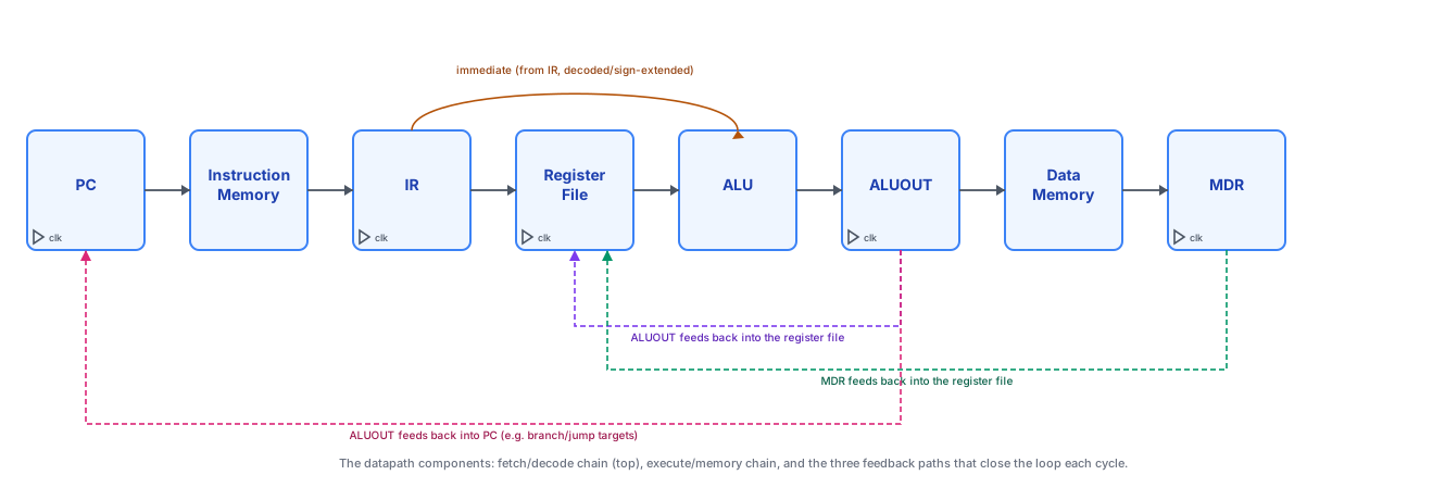
Components
- PC, IR, ALUOUT, MDR: the "extra" registers a multicycle design needs beyond the architectural register file - they hold intermediate values between cycles, so each cycle's combinational logic only needs to look at the previous cycle's results.
- Register file: from M02A01 - 32 x 32-bit,
x0hardwired to 0. Typically one write port, one or two read ports. - ALU: the same kind of module as M01A01's
alu1, but wider (32-bit) and with more operations (add, subtract, compare, shift, AND/OR/XOR - enough to cover all RV32I ALU ops). - Instruction memory / data memory: for Project 1, can start as simple synchronous-read
logicarrays (BRAM-friendly) - see M01A04 for resource budget.
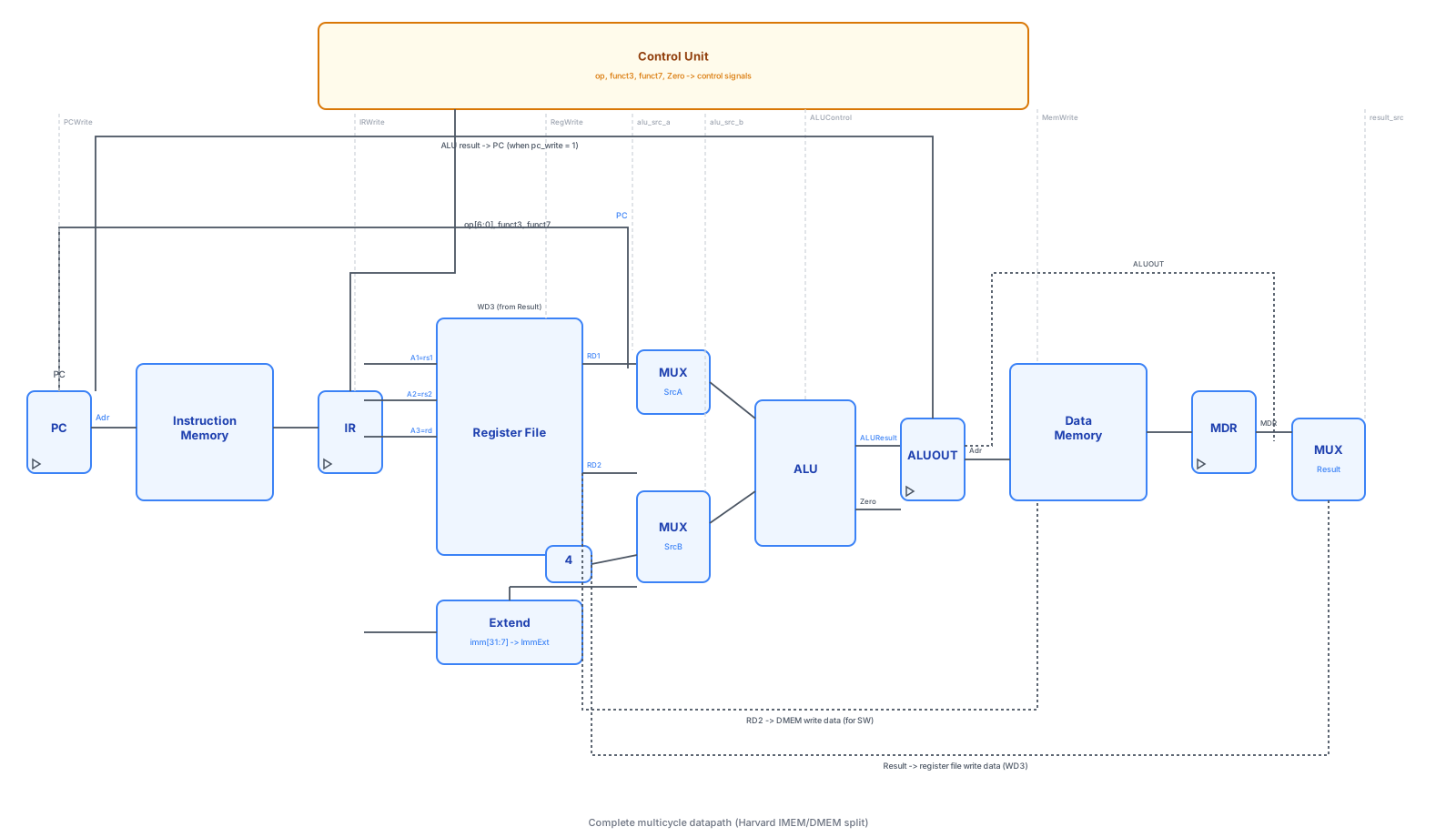
Complete multicycle datapath
Why the extra registers?
Consider LW rd, imm(rs1): address = rs1 + imm (an ALU operation), then mem[address] (a memory operation), then rd = mem[address] (a register write) - three operations that each take one cycle.
- Without
alu_outandmdr, the address computed in cycle 3 would be lost by cycle 4 - it exists only as a combinational signal during cycle 3. - This is the register + combinational logic pattern from M01A02, applied at the datapath level: every value that must survive to a later cycle needs its own register.
Control signals: the datapath's knobs
The datapath components don't decide anything by themselves - they're driven by control signals that the FSM (M02A03) sets each cycle:
| Signal | Controls |
|---|---|
pc_write |
Does PC update this cycle? |
ir_write |
Does the instruction register latch the fetched word? |
alu_op |
Which operation does the ALU perform? |
alu_src_a, alu_src_b |
What feeds the ALU's inputs (register, immediate, PC, constant 4)? |
mem_read, mem_write |
Access data memory this cycle? |
reg_write, reg_dst, result_src |
Write the register file this cycle, and from where? |
- Each signal is one bit (or a small
enum) computed byalways_combin the control FSM, based on the currentstateand the decodedopcode/funct3/funct7. - This is the same
enum+always_comb+casepattern from M01A02's FSM example - just with many more outputs per state.
Control signals per state — reference table
The FSM sets these signals on every clock cycle. A – means "don't care / unchanged":
| State | pc_write |
ir_write |
alu_src_a |
alu_src_b |
alu_op |
mem_read |
mem_write |
reg_write |
result_src |
|---|---|---|---|---|---|---|---|---|---|
| FETCH | 1 | 1 | PC | 4 | ADD | IMEM | 0 | 0 | – |
| DECODE | 0 | 0 | – | – | – | 0 | 0 | 0 | – |
| EXEC_R | 0 | 0 | RS1 | RS2 | funct7/3 | 0 | 0 | 0 | – |
| EXEC_I | 0 | 0 | RS1 | IMM | funct3 | 0 | 0 | 0 | – |
| EXEC_BRANCH | cond | 0 | RS1 | RS2 | SUB | 0 | 0 | 0 | – |
| MEM_ADDR | 0 | 0 | RS1 | IMM | ADD | 0 | 0 | 0 | – |
| MEM_READ | 0 | 0 | – | – | – | DMEM | 0 | 0 | – |
| MEM_WRITE | 0 | 0 | – | – | – | 0 | DMEM | 0 | – |
| WRITEBACK_ALU | 0 | 0 | – | – | – | 0 | 0 | 1 | ALUOUT |
| WRITEBACK_MEM | 0 | 0 | – | – | – | 0 | 0 | 1 | MDR |
pc_write = condinEXEC_BRANCHmeans "write PC only if the branch condition is true."- This table is the specification for your Project 1 control FSM — each row becomes one
casearm inalways_comb. - Signals left as
–can keep their default value (set at the top ofalways_comb) — same discipline as the accidental-latch fix from M01A02.
Putting it together: one ALU input mux
alu_src_a/alu_src_bare control signals set by the FSM. The same physical ALU computesrs1 + rs2(forADD),rs1 + imm(forLW's address),PC + imm(forBEQ's target), andPC + 4(for the next-PC default) - just by changing what feeds it.- This is the heart of "multicycle": one ALU, reused across cycles for different purposes, instead of separate adders for each.
Instruction trace: ADD x3, x1, x2
Cycle-by-cycle walk-through (4 cycles total):
| Cycle | State | Key datapath action | What updates |
|---|---|---|---|
| 1 | FETCH | IR ← mem[PC]; PC ← PC+4 via ALU |
IR, PC |
| 2 | DECODE | read rs1=x1, rs2=x2; decode R-type; state_next = EXEC_R |
(combinational) |
| 3 | EXEC_R | ALU computes x1 + x2; result → ALUOUT |
ALUOUT |
| 4 | WRITEBACK_ALU | x3 ← ALUOUT; state_next = FETCH |
register file |
Control signals in cycle 3: alu_src_a=RS1, alu_src_b=RS2, alu_op=ADD, reg_write=0 (not yet).
Control signals in cycle 4: reg_write=1, result_src=ALUOUT, reg_dst=rd.
Every R-type and I-type ALU instruction follows this exact 4-cycle template. The FSM reuses the same states — only the
alu_opand the source ofalu_src_bdiffer.
Instruction trace: LW x3, 8(x1)
The most complex instruction — 5 cycles:
| Cycle | State | Key datapath action | What updates |
|---|---|---|---|
| 1 | FETCH | IR ← mem[PC]; PC ← PC+4 |
IR, PC |
| 2 | DECODE | read rs1=x1; sign-extend imm=8; state_next = MEM_ADDR |
(combinational) |
| 3 | MEM_ADDR | ALU: x1 + 8 → ALUOUT (the load address) |
ALUOUT |
| 4 | MEM_READ | MDR ← data_mem[ALUOUT] |
MDR |
| 5 | WRITEBACK_MEM | x3 ← MDR; state_next = FETCH |
register file |
MEM_ADDRis shared withSW— both computers1 + imm; the next state distinguishes load from store.MDR(Memory Data Register) exists precisely so the loaded value survives from cycle 4 to cycle 5.- Without
MDR,data_memoutput would need to remain stable for two cycles — which is harder to guarantee and wastes a memory port.
In-class exercise — datapath trace
Exercise (10 min): trace SW x2, 12(x1) (store x2 to address x1 + 12) through the datapath.
Fill in the table:
| Cycle | State | Key datapath action | What updates |
|---|---|---|---|
| 1 | |||
| 2 | |||
| 3 | |||
| 4 |
Questions:
1. Which control signals differ from LW in cycles 3–4?
2. Does reg_write ever go high during SW? Why or why not?
3. Why does SW use only 4 cycles while LW uses 5?
Expected: FETCH → DECODE → MEM_ADDR (
x1+12→ ALUOUT) → MEM_WRITE (data_mem[ALUOUT] ← x2).reg_writeis never 1 — stores write memory, not registers. No WRITEBACK state needed.
Next class
Designing the Control FSM: the enum of states, the case-based control logic that drives every signal from the table above, and a cycle-by-cycle trace of ADDI, LW, and BEQ through the datapath.