Digital Building Blocks
Rodolfo Azevedo
Institute of Computing, University of Campinas (UNICAMP), Brazil
rodolfo.azevedo@unicamp.br
http://www.ic.unicamp.br/~rodolfo/mo801
Goal of this class
Module 1, Class 5: ALU, register file, memory arrays — and parameterized/generated modules.
Today we assemble the components of the RV32I datapath before we formally introduce RISC-V. By the end of this class, you will have seen every hardware module that Project 1 requires — what remains is wiring them together and adding the control FSM.
At the end of this class, you should be able to:
- Implement adders, an ALU with shift and comparison operations, and a barrel shifter in SystemVerilog.
- Design a register file with simultaneous read ports and a write port.
- Use parameterized modules and
generateconstructs to create scalable hardware structures. - Describe synchronous memory arrays in SystemVerilog and explain how BRAM inference works.
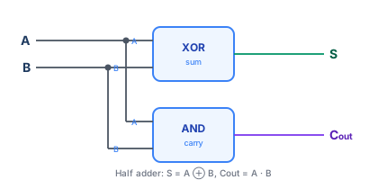
Arithmetic: half adder
A half adder adds two 1-bit values:
Full adder
A full adder also accepts a carry-in:
Ripple-carry adder
Chain \(N\) full adders to add two \(N\)-bit numbers:
The critical path runs through all \(N\) carry chains — \(O(N)\) delay. For 32 bits at 27 MHz this is fine; at GHz clock rates you'd need a carry-lookahead adder (\(O(\log N)\) delay).
parameter and localparam
parameter— can be overridden at instantiation:adder #(.WIDTH(8)) u0 (...).localparam— a constant derived from parameters; cannot be overridden externally.- Parameterized modules are the standard way to write reusable, width-independent components.
parameter WIDTH = 32is in almost every datapath module you will write.
generate — repetitive instantiation
generate for instantiates or assigns hardware in a loop that is unrolled at compile time:
Rules:
* genvar is only visible inside the generate block.
* The loop index i must be a constant expression — it is elaborated (evaluated) at compile time, not at runtime.
* Each iteration creates a separate hardware instance, named mux_array[0].m, mux_array[1].m, etc.
* Use generate when you find yourself copy-pasting the same instantiation with different indices.
The ALU
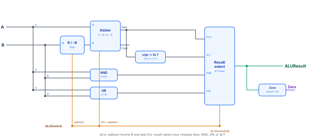
The RV32I ALU performs: ADD, SUB, AND, OR, XOR, SLT (set-less-than), SLL/SRL/SRA (shifts):
ALU code
$signed(a) >>> b is the arithmetic right shift — fills with the sign bit rather than zeros. SRA is the only arithmetic shift; the others are logical.
Barrel shifter
A barrel shifter shifts by any amount in a single cycle — required by RV32I's SLL, SRL, and SRA instructions:
$clog2(32) = 5, soshamtis a 5-bit field — matchinginstr[24:20]in RV32I I-type exactly.<<and>>are logical — vacated bits become 0.>>>on a$signedoperand is arithmetic — vacated bits copy the sign bit.
Yosys synthesises this as a cascade of 5 conditional 2:1 MUXes (one per shift-amount bit). Depth is \(O(\log_2 N)\) — a 32-bit shift costs only 5 MUX levels, not 32.
Register file
The RV32I register file: 32 registers × 32 bits, two read ports (combinational), one write port (clocked):
$clog2(REGS)— ceiling of \(\log_2(32) = 5\) — the number of bits needed to address 32 registers.- Register
x0is hardwired to zero — read always returns 0, writes are ignored. Implemented by the(ra == '0) ? '0 :guard on reads andwa != '0guard on writes.
Memory arrays: ROM and SRAM
- Asynchronous read (combinational):
assign rdata = mem[addr]— uses LUTs on the FPGA (distributed RAM). Limited size. - Synchronous read (registered):
rdata <= mem[addr]insidealways_ff— maps to BRAM on the GW1NR-9C. The Tang Nano 9K has ~468 Kbit of BRAM — far more efficient for large memories. - For the instruction memory in Project 1, use synchronous read BRAM to save LUTs for logic.
BRAM inference pitfalls
Yosys maps a synchronous-read array to dedicated BSRAM blocks. Two coding patterns silently break this and cause Yosys to fall back to thousands of LUTs:
Pitfall 1: async reset in the same process as array writes
BRAM inference pitfalls
Pitfall 2: writing multiple memories in a single if/else chain
yosys -p "synth_gowin ... stat" on the module alone. If a memory that fits in 1–2 BRAMs shows 1000+ LUTs, a pitfall was triggered.
$signed() pitfall: zero-extend vs. sign-extend
$signed() reinterprets a bit vector as a signed (two's complement) value. A subtle bug arises when prepending a bit:
- Rule: apply
$signed()to the original narrower signal, not after concatenation. - This same pitfall appears in C:
(int32_t)(uint8_t)xzero-extends;(int32_t)(int8_t)xsign-extends.
Resource implications on the Tang Nano 9K
| Component | Typical resource | Tang Nano 9K budget |
|---|---|---|
| 32×32 register file (async read) | ~64 LUTs | 8,640 LUTs total |
| 32×32 register file (sync read) | 2 BRAM blocks | 26 BRAM blocks total |
| 32-bit ALU | ~50 LUTs | (varies with operations) |
| 4 KB instruction memory (BRAM) | 1 BRAM block | 26 BRAM blocks total |
| RV32I control FSM | ~20–40 LUTs | (state + combinational) |
| Full minimal RV32I core | ~300–500 LUTs | well within budget |
The register file and memories are the largest pieces. Use BRAM for memories; use distributed RAM or LUTs for the register file (it is small enough).
In-class exercise — Yosys resource estimation
Before synthesizing, estimate the LUT cost of each module, then run Yosys and compare:
| Module | Estimated LUTs | Yosys LUT4: count |
Ratio |
|---|---|---|---|
mux2 #(32) — 32-bit 2:1 MUX |
|||
barrel_shift #(32) — all three modes |
|||
alu #(32) — ADD/SUB/AND/OR/XOR/SLT/SLL/SRL/SRA |
|||
regfile — 32×32, async read |
Discussion questions:
1. Which module uses the most LUTs? Does that match your intuition?
2. The full RV32I core uses roughly 300–500 LUTs. How much headroom is left on the Tang Nano 9K (8,640 LUTs total) for the accelerator in Project 3?
3. Run with synth_gowin -retime — does the LUT count change? Why or why not?
Preview: these are Project 1's components
You now have all the hardware you need for the RV32I multicycle core:
| Module | Purpose | Covered in |
|---|---|---|
adder / alu |
Arithmetic and logic operations | This class |
regfile |
32 × 32-bit register storage | This class |
sram |
Instruction and data memory | This class |
mux2 / mux4 |
Datapath input selection | M01A02 |
register |
IR, PC, MDR, ALUOUT pipeline registers | M01A03 |
| Control FSM | Generate all control signals | M01A04 |
Module 2 will introduce the RV32I ISA and show you exactly how to connect these components. Project 1 is the wiring and the control FSM — not new hardware primitives.
Next class
Verification & Toolchain: writing Verilator testbenches, reading VCD waveforms in GTKWave, and the full OSS CAD Suite flow from SystemVerilog source to bitstream on the Tang Nano 9K — everything you need to test and deploy Project 1.