Integration & Project 2
Rodolfo Azevedo
Institute of Computing, University of Campinas (UNICAMP), Brazil
rodolfo.azevedo@unicamp.br
http://www.ic.unicamp.br/~rodolfo/mo801
Goal of this class
Module 3, Class 4: top-level integration, end-to-end verification, and running KWS for the first time.
All the pieces exist. Today we wire them together, verify end-to-end, and run the first version of the KWS inference kernel on hardware you built. It will be slow — that is the point. Measuring how slow is what motivates Project 3.
At the end of this class, you should be able to:
- Integrate the processor, bus, and peripherals into a complete SoC top-level SystemVerilog module.
- Verify end-to-end SoC operation with compiled C programs in Verilator simulation.
- Run the KWS inference kernel on the Tang Nano 9K and observe inference results via UART.
- Measure baseline inference latency to establish the optimization target for Project 3.
Top-level integration
The full platform for Project 2:
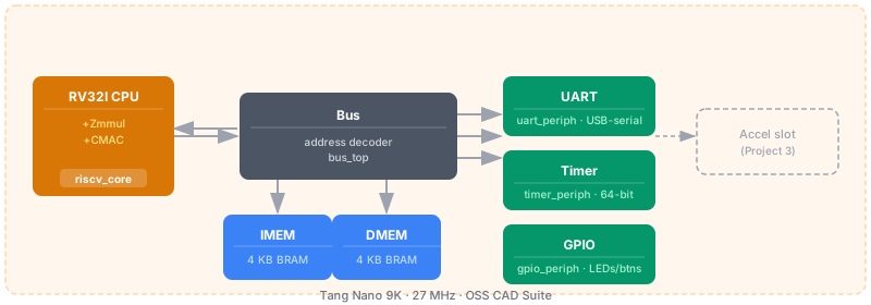
The top-level SV module instantiates: riscv_core, bus_top, uart_periph, timer_periph, gpio_periph, instruction BRAM, data BRAM.
Top-level SystemVerilog
Verification strategy: bottom-up
Build confidence layer by layer before integration:
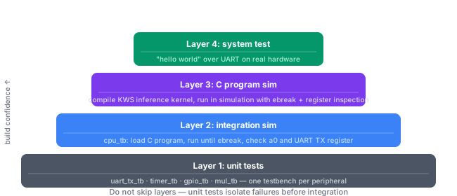
Do not skip layers. If Layer 2 fails and you have not done Layer 1, you have no idea which peripheral is broken. Unit tests isolate the failure.
Unit testbench pattern: UART TX
Open uart_tx.vcd in GTKWave and verify: start bit = 0, 8 data bits LSB-first, stop bit = 1, each lasting 234 cycles.
Integration testbench: C program on the CPU
The $write trick lets you see UART output in the simulation log without needing a full UART model.
The new loading workflow
Once the bootloader is in BRAM and the UART works on hardware, the development loop changes completely:
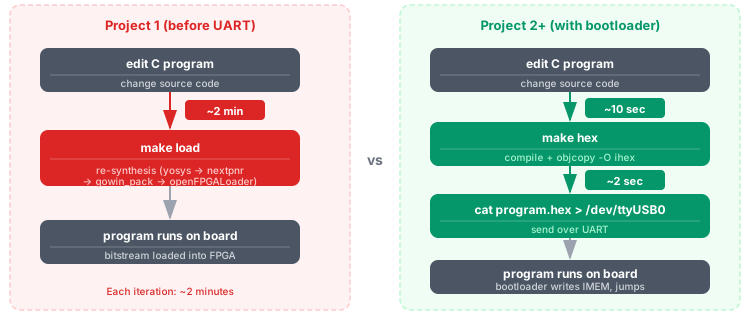
The bitstream (hardware) stays the same — only the software changes. Re-synthesis is only needed when you modify the SystemVerilog.
Running KWS for the first time
Once the platform works for "hello world", compile the KWS inference kernel:
The kernel:
1. Reads MFCC features from a lookup table in DMEM.
2. Runs the Conv2D inference layers.
3. Outputs the predicted class over UART.
4. Writes cycle counts to a buffer, then ebreak.
Expected result at this stage: it works, but it is slow — on the order of tens of millions of cycles (seconds at 27 MHz). Record the exact number. This is your baseline for Project 3.
Synthesis and resource report
After simulation passes, synthesize the full platform:
Read the nextpnr output carefully:
Key observations: * Project 2 uses ~27% of slices — plenty of room for Project 3's accelerator. * Two DSP blocks used for Zmmul and CMAC — DSPs are much faster than LUT-based multipliers. * BRAM: 4 blocks for IMEM + DMEM. 22 blocks remain for the accelerator's local buffers.
Project 2 checklist
Before submitting, verify:
- IMEM é SRAM gravável (não ROM) — bootloader pode escrever nela.
- Bootloader recebe um Intel HEX via UART, escreve em IMEM e salta para
0x0100. - Zmmul (MUL, MULH, MULHU, MULHSU) passes all directed tests in simulation.
- CMAC instruction accumulates correctly;
csrr/csrwonmaccCSR works. - Bus routes transactions to all peripherals correctly (assert
sel_*signals). - UART TX sends a known byte in simulation (GTKWave: verify start/data/stop bits).
- Timer counter increments correctly (read at \(t_0\), wait \(N\) cycles, read at \(t_1\), check \(t_1 - t_0 = N\)).
- GPIO writes turn LEDs on/off in hardware.
- C program "hello world" appears on UART terminal on the board.
- KWS inference kernel runs and produces a correct classification in simulation.
- Synthesis report: no timing violations at 27 MHz; LUT/FF/BRAM utilization recorded.
- Security: identify one security vulnerability in your design and describe how you would mitigate it.
The slides that follow cover security, energy, and reproducibility. The security corners are required reading — one of them is directly referenced in the Project 2 checklist. The energy corners are optional enrichment.
Security corner: the UART bootloader attack surface
Your bootloader accepts Intel HEX data over UART and writes it directly into IMEM. There is no authentication, no encryption, and no integrity check.
Anyone with physical access to the serial port can:
- Inject arbitrary code — send a crafted
.hexfile that overwrites the entire program. - Exfiltrate data — load a program that reads DMEM and sends it back over UART.
- Brick the device — overwrite the bootloader itself (if IMEM includes the bootloader code).
Real-world parallel
This is exactly how IoT devices get compromised: a UART console left exposed on a production PCB (often labeled TX/RX on the board) gives an attacker full control. In 2020, researchers compromised a popular home router by soldering wires to its UART pads and loading a modified firmware.
Security corner: secure boot — what a real system does
A secure boot chain prevents unauthorized code from running:
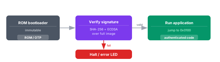
| Component | Your Project 2 | Production system |
|---|---|---|
| Boot code location | Writable SRAM | Immutable ROM |
| Code authentication | None | ECDSA / RSA signature |
| Integrity check | ihex checksum (per-line) | SHA-256 over entire image |
| Encryption in transit | None (plaintext UART) | AES-encrypted payload |
| Anti-rollback | None | Monotonic version counter in OTP fuse |
What you could add (conceptually)
- HMAC verification: compute HMAC-SHA256 of the received binary using a key stored in BRAM. If the HMAC does not match the last 32 bytes of the payload, do not jump to
0x0100. - Lock IMEM after boot: a one-way latch register — once the bootloader sets
imem_locked = 1, no further writes to IMEM are accepted until the next reset.
Security corner: memory-mapped I/O without access control
Every peripheral in your memory map is accessible from any code:
- A bug in application code could accidentally write to the UART TX register, sending garbage to the serial port.
- A compromised application could reprogram the timer to fire interrupts at maximum rate, causing a denial-of-service.
The defense: bus firewalls
In production SoCs, a bus firewall (or TrustZone on Arm) restricts which masters can access which address ranges. RISC-V's PMP can enforce this at the CPU level:
- Only machine-mode code can access I/O registers.
- User-mode code gets an access fault if it tries to write to
0x0002_xxxx.
Project 2 security question: "Your bootloader has no authentication. Describe a practical attack that exploits this and one mechanism that would prevent it."
Energy corner: peripheral power and idle management (Optional)
Every peripheral you added in Project 2 consumes power — even when idle:
| Peripheral | Idle behavior | Power impact |
|---|---|---|
| UART TX | Shift register holds 1 (mark) |
Minimal — no toggles |
| UART RX | Oversampling counter runs continuously | Clock toggles 16× per bit period, even when no data arrives |
| Timer | 64-bit counter increments every cycle | 64 flip-flops toggle every clock edge |
| GPIO | Output latches hold last value | Minimal |
The real cost: the bus
The bus routes every load/store through the address decoder, even when the target is DMEM (the most common case). Every bus transaction toggles the mux/decoder logic for all peripherals, not just the target.
In production SoCs: * Clock gating per peripheral: disabled peripherals consume zero dynamic power. * Power domains: entire peripheral blocks can be powered off (not just clock-gated). * Bus isolation: inactive peripherals are disconnected from the bus to reduce capacitive load.
Measuring power on the Tang Nano 9K
You can measure your design's power with a USB power meter:
- Baseline (FPGA configured, no design): ~80 mA at 5V
- Your Project 2 system: measure it! Compare with Project 1 — the difference is the cost of your peripherals.
Energy corner: UART baud rate and energy
A faster baud rate sends the same data in less time — but does it save energy?
- Transmit energy per byte ≈ constant (same number of bit transitions regardless of speed).
- System energy during transfer decreases at higher baud rates: the CPU waits fewer cycles polling the UART status register → fewer clock cycles → less total energy.
- At 115200 baud, sending 1 KB takes ~89 ms. At 9600 baud, it takes ~1.07 s. The CPU runs for 12× longer at the slower rate.
For the bootloader, higher baud rate is strictly better: same data, less waiting, less energy.
Reproducibility note: memory map as a contract
Your memory map (M03A01) is a hardware/software contract:
- Document it in your README — the C driver code depends on these addresses.
- Use
#defineor a header file for all addresses — never hardcode0x00020000in driver code. - Version it: if the memory map changes between Project 2 and Project 3, the old C code must not compile silently with wrong addresses.
A mismatch between the memory map in hardware and in software is one of the hardest bugs to find — everything synthesizes, everything compiles, but loads/stores go to the wrong peripheral.
Next module
Module 4 — TinyML on the Edge: the KWS model in depth, the inference kernel in C, and profiling — finding exactly which operation is responsible for the baseline cycle count we just measured.